LED Cube/PCB Soldering Manual: Unterschied zwischen den Versionen
Marvin (Diskussion | Beiträge) |
Marvin (Diskussion | Beiträge) (pcb soldering manual) |
||
| (58 dazwischenliegende Versionen desselben Benutzers werden nicht angezeigt) | |||
| Zeile 1: | Zeile 1: | ||
{{ | {{LED Cube Series/en}} | ||
This | This is the first siginificant part of the LED Cube Series. You will learn where to place the components on the PCB (Printed Circuit Board) and how solder them. | ||
<gallery widths=300 heights=200 perrow=3> | |||
File:Lcpcb-base.jpg|plain PCB | |||
</gallery> | |||
==USB Resistors== | |||
First we solder the resistors R10, R11 and R13. Here is the section of the schematic diagram containing three parts: | |||
<gallery widths=400 heights=200 > | |||
File:cube-usb.png|USB section of the schematics. | |||
</gallery> | |||
As all resistors we are going to use in this project, their orientation is not relevant. You can see the resistor values in the schematic or in the table below, together with the color code marking: | |||
{|class="wikitable" | {|class="wikitable" | ||
|- | |- | ||
!Name!!Value!!Color Code | !Name!!Value!!Color Code | ||
|- | |- | ||
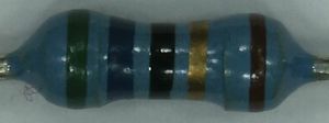
|R10||68 Ohm||[[File:r-68.jpeg|frameless|border]] | |R10||68 Ohm||[[File:r-68.jpeg|frameless|border]]<br />blue-green-black-gold-brown | ||
|- | |- | ||
|R11||68 Ohm||[[File:r-68.jpeg|frameless|border]] | |R11||68 Ohm||[[File:r-68.jpeg|frameless|border]]<br />blue-green-black-gold-brown | ||
|- | |- | ||
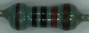
|R13||1500 Ohm||[[File:r-1500.jpeg|frameless|border]] | |R13||1500 Ohm||[[File:r-1500.jpeg|frameless|border]]<br />brown-green-black-brown-brown | ||
|} | |} | ||
<gallery perrow= | Get the resistors from your kit. Use the data above to assign them to the correct place on the PCB. If you are not sure about this, have a look at the pictures below. Then bend both leads about 90 degrees, so they fit into the two holes. The distance between the leads, as with every resistor we will solder on this board, is about 11 mm, but it is not important to be very accurate here. Place them into the holes and flip the PCB. | ||
<gallery perrow=2 widths=300 heights=200> | |||
File:lcpcb-00-00.jpg|the three resistors | File:lcpcb-00-00.jpg|the three resistors | ||
File:lcpcb-00-01.jpg|If you want to be accurate, make sure the distance between the bends is 11 mm. | File:lcpcb-00-01.jpg|If you want to be accurate, make sure the distance between the bends is 11 mm. | ||
File:lcpcb-00-02.jpg| | File:lcpcb-00-02.jpg|PCB with placed resistors | ||
File:lcpcb-00-03.jpg| | File:lcpcb-00-03.jpg|flipped PCB | ||
</gallery> | |||
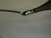
To solder them, get your already heated soldering iron, clean it with a moist sponge or the tools that available. Apply a very small amount of solder to the tip - just enough so that there is a small film on it (watch [http://www.youtube.com/watch?v=7lmCSkGZz3Q (youtube)] for reference). We will need this solder only for the iron to be able to heat up the PCB and the resistors - we will add more solder later. | |||
{{attention|An additional effect of the tin is that it protects the tip from corrosion. After you completely removed the tin from your tip by cleaning it with a moist sponge, you have to reapply solder as soon as possible afterwards. This will ensure a long tip lifetime.}} | |||
<gallery perrow=3 widths=184 heights=130> | |||
File:lcpcb-00-06.jpg|dirty tip | |||
File:lcpcb-00-07.jpg|tip after cleaning with a moist sponge | |||
File:lcpcb-00-08.jpg|tip after applying some solder | |||
</gallery> | |||
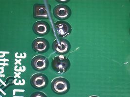
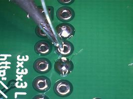
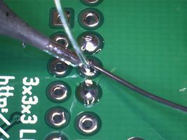
Take the soldering iron into your lead hand. Grab some solder wire with the other one. Now take the tip of the soldering iron to one of the holes where the wires of the resistor are inserted. Place the soldering iron there, for about 1 to 3 seconds to allow the PCB and the resistor lead to heat up. Then add some solder wire to the point where the tip of the soldering iron, the wire and the hole in the PCB meet until the hole is completely covered. Some of the solder will flow through the hole to the other side of the PCB. If this is the case, add more solder until you have a nice solder joint. This joint should be shiny and look like the one in the picture below: | |||
<gallery perrow=2 widths=300 heights=200> | |||
File:lcpcb-00-10.jpg|candidate for soldering | |||
File:lcpcb-00-11.jpg|correctly positioned soldering iron tip | |||
File:lcpcb-00-12.jpg|position where the solder should be added | |||
File:lcpcb-00-13.jpg|while adding solder | |||
File:lcpcb-00-14.jpg|solder joint after cooling | |||
</gallery> | |||
Repeat this for the other five joints. Afterwards, clip away any excess wire, but do not damage the solder joint by clipping away more than necessary. | |||
<gallery perrow=2 widths=300 heights=200> | |||
File:lcpcb-00-04.jpg|backside after soldering | File:lcpcb-00-04.jpg|backside after soldering | ||
File:lcpcb-00-05.jpg|after clipping away the excess leads | File:lcpcb-00-05.jpg|after clipping away the excess leads | ||
| Zeile 29: | Zeile 57: | ||
==USB Zener Diodes== | ==USB Zener Diodes== | ||
Additionally, we need two 3.6 V Zener diodes for the data lines, Z1 and Z2. Here, you have to pay attention to their orientation. The (black) line on the diode is the same as the single line on the symbol (as opposed to the triangle) that is printed onto the PCB. You can see that in this figure: | |||
Additionally, we need two 3.6 V Zener diodes for the data lines, Z1 and Z2. Here, you have to pay attention to their orientation. The (black) line on the diode is the same as the single line on the symbol (as opposed to the triangle) that is printed onto the PCB. You can see that in | <gallery perrow=2 widths=300 heights=200> | ||
File:Zener.jpeg|Zener diode orientation | |||
</gallery> | |||
First bend the Zener diodes, so they fit into their holes. This time the holes are only 7.5 mm apart. Then put them into their place and flip the PCB. | |||
<gallery perrow= | <gallery perrow=2 widths=300 heights=200> | ||
File:lcpcb-01-00.jpg|the two Zener diodes | File:lcpcb-01-00.jpg|the two Zener diodes | ||
File:lcpcb-01-01.jpg|this time, the distance between the leads is 7.5 mm | File:lcpcb-01-01.jpg|this time, the distance between the leads is 7.5 mm | ||
File:lcpcb-01-02.jpg|PCB with the diodes placed | File:lcpcb-01-02.jpg|PCB with the diodes placed | ||
File:lcpcb-01-025.jpg| | File:lcpcb-01-025.jpg|flipped PCB | ||
</gallery> | |||
Soldering the Zener diodes is nearly like solering the resistors, but it is a little bit more difficult. If you have a closer look at the holes, you will see two differences: | |||
# Two of them are quadratic. They can be soldered like the resistors in the previous step. | |||
# Two of them are round and look a little bit like a blossom: They are directly connected to the big copper plane on the side you are currently looking on. This is the issue: To heat up this large layer of copper will take more time than previously, so give these joints some extra time. | |||
<gallery perrow=3 widths=184 heights=130> | |||
File:lcpcb-01-05.jpg|microscropy view on the problematic hole | |||
File:lcpcb-01-03.jpg|back side after soldering | File:lcpcb-01-03.jpg|back side after soldering | ||
File:lcpcb-01-04.jpg|back side after clipping | File:lcpcb-01-04.jpg|back side after clipping | ||
| Zeile 43: | Zeile 80: | ||
==Reset Resistor== | ==Reset Resistor== | ||
<gallery widths=200 heights=200 > | |||
The Reset pin gets a 10 kOhm resistor R12 to the 5 V line. Again, have a look in the table for the correct color markings. Orientation is irrelevant. | File:cube-isp.png|Reset resistor and ISP header in the schematic diagram. (The ISP header is left unsoldered in this tutorial.) | ||
</gallery> | |||
The Reset pin of the microcontroller gets a 10 kOhm resistor R12 to the +5 V line. Again, have a look in the table for the correct color markings. Orientation is irrelevant. | |||
{|class="wikitable" | {|class="wikitable" | ||
|- | |- | ||
!Name!!Value!!Color Code | !Name!!Value!!Color Code | ||
|- | |- | ||
|R12||10 kOhm||[[File:r-10000.jpeg|frameless|border]] | |R12||10 kOhm||[[File:r-10000.jpeg|frameless|border]]<br />brown-black-black-red-brown | ||
|} | |} | ||
<gallery perrow= | |||
It should be clear how you solder this resistor. If not, have a look at the previous steps. | |||
<gallery perrow=2 widths=300 heights=200> | |||
File:lcpcb-02-00.jpg|the reset resistor... | File:lcpcb-02-00.jpg|the reset resistor... | ||
File:lcpcb-02-01.jpg|...placed and soldered | File:lcpcb-02-01.jpg|...placed and soldered | ||
| Zeile 57: | Zeile 98: | ||
==Column Resistors== | ==Column Resistors== | ||
<gallery widths=500 heights=250> | |||
If you bought a kit or attend a workshop, you probably already got the correct Resistors. There should be (at least) nine of the same value. Just solder them into the places for R1 to R9. | File:cube-columns.png|Column resistors and column connectors in the schematic diagram | ||
</gallery> | |||
If you bought a kit or attend a workshop, you probably already got the | |||
correct Resistors. | |||
There should be (at least) nine of the same value. | |||
Just solder them into the places for R1 to R9. | |||
If you are supplying your own LEDs or did not get matching resistors for any other reason, you have to pay attention: The ideal column resistors should be chosen for each LED color separately. You are always on the safe side, if you choose a high value, but then your cube may not be as bright as you want it to be. If you are interested in this, read [[LED Cube/Column Resistors in Detail]]. Alternatively, here is a table of common colors, their forward voltages and the recommended resistor value: | If you are supplying your own LEDs or did not get matching resistors for | ||
any other reason, you have to pay attention: | |||
The ideal column resistors should be chosen for each LED color separately. | |||
You are always on the safe side, if you choose a high value, but then your | |||
cube may not be as bright as you want it to be. If you are interested in | |||
this, read [[LED Cube/Column Resistors in Detail]]. Alternatively, here is | |||
a table of common colors, their forward voltages and the recommended | |||
resistor value: | |||
{|class="wikitable" | {|class="wikitable" | ||
|- | |- | ||
!Color!!Forward Voltage!!Resistor Value (nearest @15 mA)!!Color Code | !Color!!Forward<br />Voltage!!Resistor Value<br />(nearest @15 mA)!!Color Code | ||
|- | |||
|Red||1.9 V|| 120 Ohm || [[File:r-120.jpeg|frameless|border]]<br />brown-red-black-black-brown | |||
|- | |||
|Blue||3.0 V|| 56 Ohm || [[File:r-56.jpeg|frameless|border]]<br />green-blue-black-gold-brown | |||
|- | |- | ||
| | |White||3.0 V|| 56 Ohm || [[File:r-56.jpeg|frameless|border]]<br />green-blue-black-gold-brown | ||
|- | |- | ||
|} | |} | ||
<gallery perrow= | <gallery perrow=2 widths=300 heights=200> | ||
File:lcpcb-03-00.jpg|the (example) resistors... | File:lcpcb-03-00.jpg|the (example) resistors... | ||
File:lcpcb-03-01.jpg|...after bending, | File:lcpcb-03-01.jpg|...after bending, | ||
| Zeile 78: | Zeile 135: | ||
==Column and Plane Connectors== | ==Column and Plane Connectors== | ||
<gallery widths=250 heights=250> | |||
File:cube-planes.png|plane connectors (and transistor array) in the schematic diagram | |||
</gallery> | |||
Now add the column and plane connectors to CONN1 to CONN10. This step is optional and it is probably the most annoying part of this PCB, but you should think twice before you skip it: It allows you to disconnect and reconnect your cube without expensive equipment. And do repairs on it which may not be possible while it is connected. But it's your choice - skipping this step does not have any other significant effect. | Now add the column and plane connectors to CONN1 to CONN10. This step is optional and it is probably the most annoying part of this PCB, but you should think twice before you skip it: It allows you to disconnect and reconnect your cube without expensive equipment. And do repairs on it which may not be possible while it is connected. But it's your choice - skipping this step does not have any other significant effect. | ||
So, to add the connectors, we first have to separate them from the break-away header row. You can do this with a scalpel or side cutters. You will need nine single-pin connectors and one 3-pin connector. You can also completely remove the plastic around them if you want. Now put one by one into the pcb, and solder them. You do not have to cut away any excess wire afterwards. You may however try to reheat some solder joints and wiggle on them, if the connectors are not straight. | So, to add the connectors, we first have to separate them from the break-away header row. You can do this with a scalpel or side cutters. You will need nine single-pin connectors and one 3-pin connector. You can also completely remove the plastic around them if you want. Now put one by one into the pcb, and solder them. You do not have to cut away any excess wire afterwards. You may however try to reheat some solder joints and wiggle on them, if the connectors are not straight. | ||
<gallery perrow=3> | <gallery perrow=3 widths=184 heights=130> | ||
File:lcpcb-04-00.jpg|the first plane connector in the top right corner | File:lcpcb-04-00.jpg|the first plane connector in the top right corner | ||
File:lcpcb-04-01.jpg|the same connector now in the top right corner | File:lcpcb-04-01.jpg|the same connector now in the top right corner | ||
| Zeile 90: | Zeile 149: | ||
==Capacitors== | ==Capacitors== | ||
We need four capacitors, two times 100 nF (C1, C2) and two times 22 pF (C3, C4). See the schematic at the left or the table below for their values and positions. Again, all four devices are symmetric and orientation is irrelevant. | We need four capacitors, two times 100 nF (C1, C2) and two times 22 pF (C3, C4). See the schematic at the left or the table below for their values and positions. Again, all four devices are symmetric and orientation is irrelevant. | ||
To keep them near to the PCB before flipping it, bend the leads to the outside (about 10 to 20 degrees) after inserting them. | |||
[[File:cube-uc.png|thumb|350px]] | [[File:cube-uc.png|thumb|350px]] | ||
{|class="wikitable" | {|class="wikitable" | ||
| Zeile 103: | Zeile 164: | ||
|C4||22 pF||[[File:lcpcb-05-00.jpg|100px]] (220 or 22 ≙ 22 * 10^0 pF = 22 pF) | |C4||22 pF||[[File:lcpcb-05-00.jpg|100px]] (220 or 22 ≙ 22 * 10^0 pF = 22 pF) | ||
|} | |} | ||
<gallery perrow= | <gallery perrow=2 widths=300 heights=200> | ||
File:lcpcb-05-03.jpg|The PCB with the capacitors soldered into it. | File:lcpcb-05-03.jpg|The PCB with the capacitors soldered into it. | ||
</gallery> | </gallery> | ||
| Zeile 110: | Zeile 171: | ||
Now you should add the 16 MHz crystal U3. You do not have to care about its orientation. | Now you should add the 16 MHz crystal U3. You do not have to care about its orientation. | ||
<gallery> | <gallery perrow=3 widths=184 heights=130> | ||
File:Crystal.jpeg|16 MHz crystal | File:Crystal.jpeg|16 MHz crystal | ||
File:lcpcb-06-00.jpg|16 MHz crystal | File:lcpcb-06-00.jpg|16 MHz crystal | ||
| Zeile 118: | Zeile 179: | ||
==Transistor Array== | ==Transistor Array== | ||
[[File:cube-planes.png|thumb|200px]] | [[File:cube-planes.png|thumb|200px]] | ||
Now add the transistor array U2. | Now we will add the transistor array U2. | ||
<gallery perrow= | <gallery perrow=2 widths=300 heights=200> | ||
File:lcpcb-07-00.jpg| | File:lcpcb-07-00.jpg|ULN2003A | ||
</gallery> | </gallery> | ||
But first we have to make sure it fits. If you have a look at the following picture you can clearly see that the way the IC got deliviered to you, | But first we have to make sure it fits. If you have a look at the following picture you can clearly see that the way the IC got deliviered to you, it is clear that the pins are tilted too much. | ||
<gallery perrow= | <gallery perrow=2 widths=300 heights=200> | ||
File:lcpcb-07-01.jpg| | File:lcpcb-07-01.jpg|ULN2003 compared to the hole distance on the PCB | ||
</gallery> | </gallery> | ||
To get them straight, | To get them straight, grab the IC with both hands and put it on a flat surface. Then slowly bend it forward until the legs are straight. | ||
<gallery perrow= | <gallery perrow=2 widths=300 heights=200> | ||
File:lcpcb-07-02.jpg| | File:lcpcb-07-02.jpg|Bending the legs of the ULN2003A | ||
</gallery> | </gallery> | ||
| Zeile 146: | Zeile 207: | ||
[[File:cube-uc.png|thumb|350px]] | [[File:cube-uc.png|thumb|350px]] | ||
Add the microcontroller socket to the PCB at U1. As with the Transistor array, there is a small marker on the package which should be on the same side as the marker on the PCB. | Add the microcontroller socket to the PCB at U1. As with the Transistor array, there is a small marker on the package which should be on the same side as the marker on the PCB. | ||
{{SmallAttention|If the socket does not slide into the PCB and you have to apply more force than you would apply to a sharp knife while cutting onions, not all pins are pointing straight down. This is normal and you can simply take the pins and bent them until they are straight.}} | |||
<gallery perrow=3> | <gallery perrow=3> | ||
File:lcpcb-08-00.jpg|the socket | File:lcpcb-08-00.jpg|the socket | ||
| Zeile 169: | Zeile 231: | ||
File:lcpcb-10-02.jpg|In this position, the microcontroller will start the bootloader after a power-cycle. | File:lcpcb-10-02.jpg|In this position, the microcontroller will start the bootloader after a power-cycle. | ||
</gallery> | </gallery> | ||
{{continue|This was the first part of this tutorial. You should continue with [[LED Cube/Cube Soldering Manual|Section 2: Cube Soldering Manual]].}} | |||
Aktuelle Version vom 4. Mai 2012, 07:39 Uhr
| LED Cube Series | |
|---|---|
|
Chapter 1: Build Section 0: Preparation and Requirements Section 1: PCB Soldering Manual Section 2: Cube Soldering Manual Section 3: Assembly and Testing | |
|
Chapter 2: Play | |
|
Chapter 3: Learn |
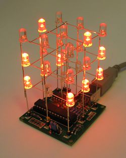
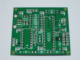
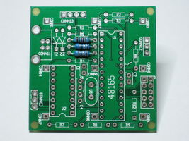
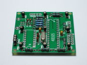
This is the first siginificant part of the LED Cube Series. You will learn where to place the components on the PCB (Printed Circuit Board) and how solder them.
-
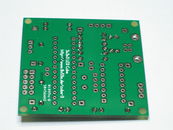
plain PCB
USB Resistors[Bearbeiten]
First we solder the resistors R10, R11 and R13. Here is the section of the schematic diagram containing three parts:
-
USB section of the schematics.
As all resistors we are going to use in this project, their orientation is not relevant. You can see the resistor values in the schematic or in the table below, together with the color code marking:
| Name | Value | Color Code |
|---|---|---|
| R10 | 68 Ohm | 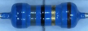 blue-green-black-gold-brown |
| R11 | 68 Ohm |  blue-green-black-gold-brown |
| R13 | 1500 Ohm | 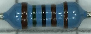 brown-green-black-brown-brown |
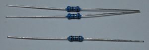
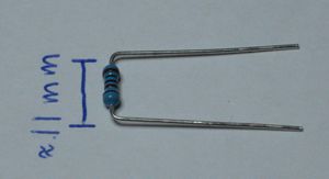
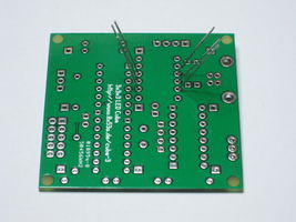
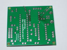
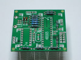
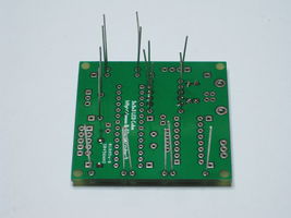
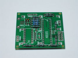
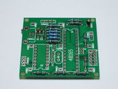
Get the resistors from your kit. Use the data above to assign them to the correct place on the PCB. If you are not sure about this, have a look at the pictures below. Then bend both leads about 90 degrees, so they fit into the two holes. The distance between the leads, as with every resistor we will solder on this board, is about 11 mm, but it is not important to be very accurate here. Place them into the holes and flip the PCB.
-
the three resistors
-
If you want to be accurate, make sure the distance between the bends is 11 mm.
-
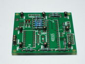
PCB with placed resistors
-
flipped PCB
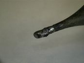
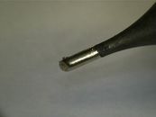
To solder them, get your already heated soldering iron, clean it with a moist sponge or the tools that available. Apply a very small amount of solder to the tip - just enough so that there is a small film on it (watch (youtube) for reference). We will need this solder only for the iron to be able to heat up the PCB and the resistors - we will add more solder later.
-
dirty tip
-
tip after cleaning with a moist sponge
-
tip after applying some solder
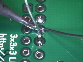
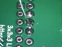
Take the soldering iron into your lead hand. Grab some solder wire with the other one. Now take the tip of the soldering iron to one of the holes where the wires of the resistor are inserted. Place the soldering iron there, for about 1 to 3 seconds to allow the PCB and the resistor lead to heat up. Then add some solder wire to the point where the tip of the soldering iron, the wire and the hole in the PCB meet until the hole is completely covered. Some of the solder will flow through the hole to the other side of the PCB. If this is the case, add more solder until you have a nice solder joint. This joint should be shiny and look like the one in the picture below:
-
candidate for soldering
-
correctly positioned soldering iron tip
-
position where the solder should be added
-
while adding solder
-
solder joint after cooling
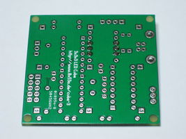
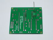
Repeat this for the other five joints. Afterwards, clip away any excess wire, but do not damage the solder joint by clipping away more than necessary.
-
backside after soldering
-
after clipping away the excess leads
USB Zener Diodes[Bearbeiten]
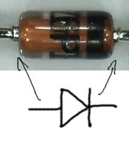
Additionally, we need two 3.6 V Zener diodes for the data lines, Z1 and Z2. Here, you have to pay attention to their orientation. The (black) line on the diode is the same as the single line on the symbol (as opposed to the triangle) that is printed onto the PCB. You can see that in this figure:
-
Zener diode orientation
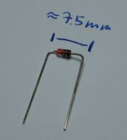
First bend the Zener diodes, so they fit into their holes. This time the holes are only 7.5 mm apart. Then put them into their place and flip the PCB.
-
the two Zener diodes
-
this time, the distance between the leads is 7.5 mm
-
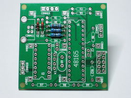
PCB with the diodes placed
-
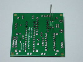
flipped PCB
Soldering the Zener diodes is nearly like solering the resistors, but it is a little bit more difficult. If you have a closer look at the holes, you will see two differences:
- Two of them are quadratic. They can be soldered like the resistors in the previous step.
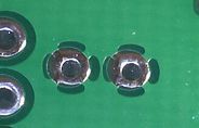
- Two of them are round and look a little bit like a blossom: They are directly connected to the big copper plane on the side you are currently looking on. This is the issue: To heat up this large layer of copper will take more time than previously, so give these joints some extra time.
-
microscropy view on the problematic hole
-
back side after soldering
-
back side after clipping
Reset Resistor[Bearbeiten]
-
Reset resistor and ISP header in the schematic diagram. (The ISP header is left unsoldered in this tutorial.)
The Reset pin of the microcontroller gets a 10 kOhm resistor R12 to the +5 V line. Again, have a look in the table for the correct color markings. Orientation is irrelevant.
| Name | Value | Color Code |
|---|---|---|
| R12 | 10 kOhm | 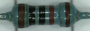 brown-black-black-red-brown |
It should be clear how you solder this resistor. If not, have a look at the previous steps.
-
the reset resistor...
-
...placed and soldered
Column Resistors[Bearbeiten]
-
Column resistors and column connectors in the schematic diagram
If you bought a kit or attend a workshop, you probably already got the correct Resistors. There should be (at least) nine of the same value. Just solder them into the places for R1 to R9.
If you are supplying your own LEDs or did not get matching resistors for any other reason, you have to pay attention: The ideal column resistors should be chosen for each LED color separately. You are always on the safe side, if you choose a high value, but then your cube may not be as bright as you want it to be. If you are interested in this, read LED Cube/Column Resistors in Detail. Alternatively, here is a table of common colors, their forward voltages and the recommended resistor value:
-
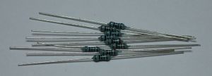
the (example) resistors...
-
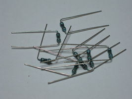
...after bending,
-
...placing, ...
-
...from the back, ...
-
...and after soldering and clipping.
Column and Plane Connectors[Bearbeiten]
-
plane connectors (and transistor array) in the schematic diagram
Now add the column and plane connectors to CONN1 to CONN10. This step is optional and it is probably the most annoying part of this PCB, but you should think twice before you skip it: It allows you to disconnect and reconnect your cube without expensive equipment. And do repairs on it which may not be possible while it is connected. But it's your choice - skipping this step does not have any other significant effect.
So, to add the connectors, we first have to separate them from the break-away header row. You can do this with a scalpel or side cutters. You will need nine single-pin connectors and one 3-pin connector. You can also completely remove the plastic around them if you want. Now put one by one into the pcb, and solder them. You do not have to cut away any excess wire afterwards. You may however try to reheat some solder joints and wiggle on them, if the connectors are not straight.
-
the first plane connector in the top right corner
-
the same connector now in the top right corner
-
after soldering of all connectors
Capacitors[Bearbeiten]
We need four capacitors, two times 100 nF (C1, C2) and two times 22 pF (C3, C4). See the schematic at the left or the table below for their values and positions. Again, all four devices are symmetric and orientation is irrelevant.
To keep them near to the PCB before flipping it, bend the leads to the outside (about 10 to 20 degrees) after inserting them.

| Name | Value | Marking |
|---|---|---|
| C1 | 100 nF | 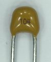 (104 ≙ 10 * 10^4 pF = 100 nF) (104 ≙ 10 * 10^4 pF = 100 nF)
|
| C2 | 100 nF |  (104 ≙ 10 * 10^4 pF = 100 nF) (104 ≙ 10 * 10^4 pF = 100 nF)
|
| C3 | 22 pF | 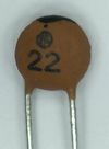 (220 or 22 ≙ 22 * 10^0 pF = 22 pF) (220 or 22 ≙ 22 * 10^0 pF = 22 pF)
|
| C4 | 22 pF |  (220 or 22 ≙ 22 * 10^0 pF = 22 pF) (220 or 22 ≙ 22 * 10^0 pF = 22 pF)
|
-
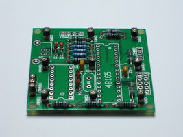
The PCB with the capacitors soldered into it.
Crystal[Bearbeiten]
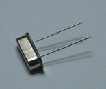
Now you should add the 16 MHz crystal U3. You do not have to care about its orientation.
-
16 MHz crystal
-
16 MHz crystal
-
PCB with crystal
Transistor Array[Bearbeiten]

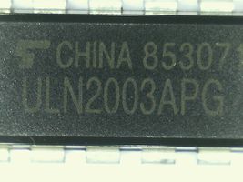
Now we will add the transistor array U2.
-
ULN2003A
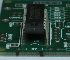
But first we have to make sure it fits. If you have a look at the following picture you can clearly see that the way the IC got deliviered to you, it is clear that the pins are tilted too much.
-
ULN2003 compared to the hole distance on the PCB
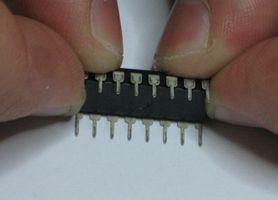
To get them straight, grab the IC with both hands and put it on a flat surface. Then slowly bend it forward until the legs are straight.
-
Bending the legs of the ULN2003A
Now you see that it fits.
Before soldering, make sure that the notches are correctly aligned. You will find one on the IC itself and one on the PCB.
Microcontroller socket[Bearbeiten]

Add the microcontroller socket to the PCB at U1. As with the Transistor array, there is a small marker on the package which should be on the same side as the marker on the PCB.
-
the socket
-
notch marker on the PCB
-
notch marker on the socket
-
PCB with socket
USB Socket[Bearbeiten]

Now add the USB socket. This should be straightforward. You should solder the two big shield connectors on the side, not just plug them in, to increase the stability.
-
the USB Socket
-
soldered (view from above)
-
soldered (view from below)
Bootloader Jumper[Bearbeiten]
Now we need the bootloader Jumper CONN12.
-
The pin header with jumper...
-
and as it is soldered.
-
In this position, the microcontroller will start the bootloader after a power-cycle.
|
This was the first part of this tutorial. You should continue with Section 2: Cube Soldering Manual. |
