LED Cube/PCB Soldering Manual: Unterschied zwischen den Versionen
Marvin (Diskussion | Beiträge) |
Marvin (Diskussion | Beiträge) Keine Bearbeitungszusammenfassung |
||
| Zeile 44: | Zeile 44: | ||
|} | |} | ||
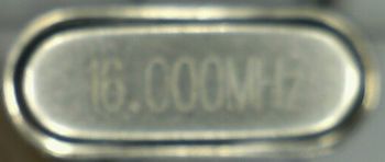
==Crystal== | ==Crystal== | ||
[[File:Crystal.jpeg]] | [[File:Crystal.jpeg|350px]] | ||
Version vom 14. April 2012, 22:22 Uhr
A full schematic of the PCB can be downloaded here: Datei:Cube.pdf.
USB Resistors

First we solder R10, R11, R13, Z1 and Z2. As all resistors we are using in this project, their orientation is not relevant. You can see the resistor values in the schematic or in the table below, together with the color code marking:
| Name | Value | Color Code |
|---|---|---|
| R10 | 68 Ohm | 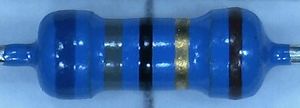
|
| R11 | 68 Ohm | 
|
| R13 | 1500 Ohm | 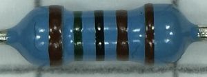
|
USB Zener Diodes
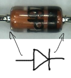
Additionally, we need two 3.6 V Zener diodes for the data lines, Z1 and Z2. Here, you have to pay attention to their orientation. The (black) line on the diode is the same as the single line on the symbol (as opposed to the triangle) that is printed onto the PCB. You can see that in the figure on the left.
Reset Resistor

The Reset pin gets a 10 kOhm resistor R12 to the 5 V line. Again, have a look in the table for the correct color markings. Orientation is irrelevant.
| Name | Value | Color Code |
|---|---|---|
| R12 | 10 kOhm | 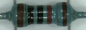
|
Column Resistors
@todo
Capacitors
We need four capacitors, two times 100 nF (C1, C2) and two times 22 pF (C3, C4). See the schematic at the left or the table below for their values and positions. Again, all four devices are symmetric and orientation is irrelevant.

| Name | Value | Marking |
|---|---|---|
| C1 | 100 nF | 104 |
| C2 | 100 nF | 104 |
| C3 | 22 pF | 220 |
| C4 | 22 pF | 220 |
