Drawdio: Unterschied zwischen den Versionen
Marvin (Diskussion | Beiträge) Keine Bearbeitungszusammenfassung |
Marvin (Diskussion | Beiträge) |
||
| Zeile 19: | Zeile 19: | ||
Then the orientation of this device is important. You can see a notch on the IC marker on the PCB. On the IC this side is also marked, for example by a dot or a thick line. | Then the orientation of this device is important. You can see a notch on the IC marker on the PCB. On the IC this side is also marked, for example by a dot or a thick line. | ||
Now add a little bit of tin to the upper left pad on PCB. Do this by heading up the pad with your soldering iron and ''then'' applying tin to the pad, not the tip. | # Now add a little bit of tin to the upper left pad on PCB. Do this by heading up the pad with your soldering iron and ''then'' applying tin to the pad, not the tip. | ||
# Grab the IC with your tweezers in your lead hand. Grab the soldering iron with your other hand. Heat up the pad you just added solder to and then place the IC correctly onto the PCB. It should now be held in place by the one solder joint, even if this joint does not look very nice right now. | |||
# Solder all other joints, one by one. | |||
# Heat up the first joint and add a little bit of solder. The joint should then look nice and shiny. | |||
===Rectifier Diode=== | |||
To protect your drawdio from anybody who tries to insert the battery in reverse, add a diode of type 4N400x (wher the x can be anything from 1 to 7). Again, the place is marked with D1. On the PCB, you will also see a diode sign. This sign can be decomposed into a triangle and a single line. | |||
[[Category:Projekte]] | [[Category:Projekte]] | ||
[[Category:Bausaetze]] | [[Category:Bausaetze]] | ||
Version vom 12. Mai 2012, 19:39 Uhr


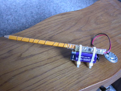
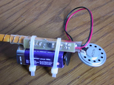
This Drawdio is a clone of the famous Drawdio by Jay Silver. This design is optimized to be cheap enough and have a component orientation that makes soldering quite easy, so you can train soldering SMT components for the first time. This the Drawdio accompanies our SMT soldering workshop.
Schematic
Getting the Design Data
You can checkout the git repository with the gschem schematics and geda pcb board file:
git clone http://www.0x53a.de/git/drawdio
Building Tutorial
555 Timer
We start with soldering the 555 Timer IC. For this, first think about how it has to be placed on the PCB. The area should be relatively easy to determine, you can do this either by the form of the pads where the legs will be soldered to or by the name: The place is marked "U1".
Then the orientation of this device is important. You can see a notch on the IC marker on the PCB. On the IC this side is also marked, for example by a dot or a thick line.
- Now add a little bit of tin to the upper left pad on PCB. Do this by heading up the pad with your soldering iron and then applying tin to the pad, not the tip.
- Grab the IC with your tweezers in your lead hand. Grab the soldering iron with your other hand. Heat up the pad you just added solder to and then place the IC correctly onto the PCB. It should now be held in place by the one solder joint, even if this joint does not look very nice right now.
- Solder all other joints, one by one.
- Heat up the first joint and add a little bit of solder. The joint should then look nice and shiny.
Rectifier Diode
To protect your drawdio from anybody who tries to insert the battery in reverse, add a diode of type 4N400x (wher the x can be anything from 1 to 7). Again, the place is marked with D1. On the PCB, you will also see a diode sign. This sign can be decomposed into a triangle and a single line.